

|
Electron Gun |
200 kV Schottky Field Emission |
|
Magnification |
TEM 8 x - 1,000,000 x STEM 2,000 x - 5,000,000 x |
|
|
Illumination |
Kohler type (4 lenses) |
|
Spectrometer |
In-column corrected Omega filter |
|
|
Objective lens |
HR, f=1.7 mm, Cs=1.2 mm, Cc=1.2 mm |
|
Energy Resolution |
≤ 0.7 eV |
|
|
Detector |
2k x 2k SS-CCD |
|
Specimen Stages |
Analytical double tilt holder ±30° / ±30° |
|
|
Spatial Resolution |
Point Resolution: |
0.24 nm |
|
|
Cryo single tilt holder ±30° |
|
Information Limit: |
0.14 nm |
|
|
Tomographic dual-axis holder ±60° |
|
|
STEM Resolution: |
0.3 nm |
|
|
|
|
Research Scientists


Dr. Laura Polito - PhD
laura.polito@scitec.cnr.it


Discover the fine morphology and structure of your nanomaterial!
Find out the elemental composition and maps at nanoscale!

High Z-contrast images through STEM

Crystalline structure characterization with nano and electron diffraction SAED

HRTEM Imaging
High-resolution transmission electron microscopy (HRTEM) is an imaging mode of the transmission electron microscope (TEM) that allows the imaging of the crystallographic structure of a specimen at atomic level. This operation mode is a powerful tool to achieve information about the local structural properties of nanostructured materials such as crystalline phases, orientation. Moreover, it can be effectively combined with a deep analytical characterization. LIBRA ZEISS 200 FE instrument lead to a point resolution of 0.24 nm and a maximum magnification 1000000x.


Analytic at nanoscale
Energy Dispersive X-Ray Analysis (EDX), is an non-destructive analytical technique used to identify the elemental atomic composition of nanostructured materials by means characteristic X-rays emitted after the interaction of the electron beam with the specimen. This technique provides spatially resolved chemical composition in 1D (line profile) or 2D (elemental map).
Electron Energy-Loss spectroscopy (EELS) is the analysis of the energy distribution of the incident electrons beam after the interaction with thin specimen ( ≤ 200nm). The energy-loss is peculiar of an electron shell of a specific element. This technique allows identifying all the elements of the periodic table (including lighter ones) and quantify them. Moreover, the oxidation state of the elements and the sample thickness can be determined.
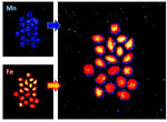
Energy-filtered transmission electron microscopy (EFTEM) is a technique used in Transmission electron microscopy, in which only electrons of particular kinetic energies are used to form the image or diffraction pattern. The technique can be used to aid chemical analysis of the sample in conjunction with complementary techniques such as electron crystallography. Here on the left ESI maps of MnFe2O4 where Fe and Mn are reported in red and blue respectively. The growth of these NCs starts with iron oxide seeds oated with by manganese oxide


HAADF-STEM
A scanning transmission electron microscope (STEM) is a type of TEM operational mode where the electron beam is focused into a narrow spot which is scanned over the sample in a raster. By using a STEM and a high-angle detector (HAADF), it is possible to form atomic resolution images where the contrast is directly related to the atomic number (z-contrast image), highlighting the small NPs embedded in the matrix. The crystalline-contrast of STEM mode makes easy and fast detect nano-crystal from amorphous phase.


Electron Diffraction
Electron diffraction of nanoparticles or nanocrystals gives information about crystalline phases and structure. Polycrystalline systems give ring patterns analogous to those from X-ray powder diffraction and can be used to identify texture and discriminate nanocrystalline from amorphous phases. Single crystals give dots pattern carrying information about the space group symmetries and the crystal's orientation to the beam path. Thanks to the SAED (Selected Area Electron Diffraction) analysis the diffraction information could be extracted from very small volumes in order to correlate the crystalline information with the morphological features.

